Over the past decade the increasing device performance demanded the continuous miniaturization of electronic devices down to a few nano-meter. Novel nano-materials promise a further boost in performance. However, in-depth understanding of charge transport of emerging materials is key although experimentally challenging. At these length scales the environment as well as the precise chemical composition of the junction will influence the measurement. Therefore, having utmost control over the junction is of great importance. The invention of mechanical-controllable break-junction enabled researchers to reliable address individual molecules which resulted in many ground-breaking transport experiments on the single atom/molecule level. The downside of this technique is a limited control over the fabrication process of the junction. Its precise chemical configuration is experimentally not accessible and possible structural defects/variations cannot be experimentally resolved. With the advent of scanning probe microscopy (SPM), the high spatial resolution enabled researchers not only to image materials with atomic resolution but also to manipulate individual atoms or molecules. By lifting single molecules from the surface, SPM pulling, the length dependent conductance of the molecule attached to the SPM tip is measured. This has the advantage that the structure of the molecule can be imaged before and after each transport measurement. Therefore, it is possible to directly correlate the length dependent conductance traces to the chemical composition of the molecule. However, the bent geometry of the free-standing molecule might perturb the charge transport compared to a planar geometry. Furthermore, this technique is limited to small molecule which are weakly adsorbed and can not be applied to larger materials.
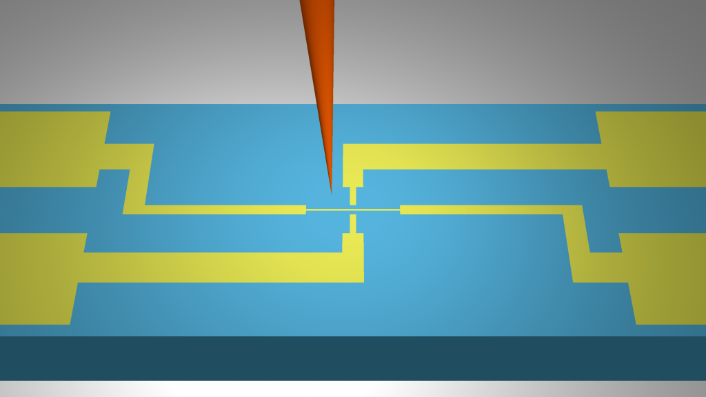
Ultra-shallow Electrodes for In-Situ Transport Experiments
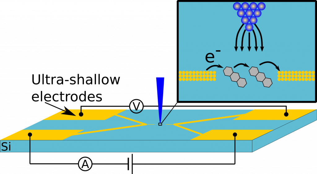
We developed a new sample architecture for SPM, where ultra-shallow electrodes are ion-implanted in an otherwise at low-temperature insulating silicon host. The here presented ultra-shallow electrodes are contacted in-situ and are used simultaneously with SPM imaging and manipulation to realize nano-scale transport and gating experiments: Molecular structures can be studied electrically while they are assembled/changed by SPM manipulation. In other words, the tip of the SPM is a mobile probe for atomic-scale characterization of the structure but at also a tool to induce structural changes to the material of interest.
STM Hydrogen Resist Lithography
Si(100), widely used for industrial applications, is a versatile substrate to study the charge transport of organic structures or 2D materials. Crucial for our research is the tunability of the chemical reactivity of the surface by partially passivating the substrate with hydrogen. This control over chemical reactivity has been used for example in STM hydrogen resist lithography to pattern preferential molecular adsorption sites for organic compounds or for atomically precise dopant placement. In a nutshell, the STM tip is used to remove the hydrogen resist with atomic precision which creates highly reactive patches on the surface. We investigate if this technique can be used to bind otherwise mobile molecules and to steer self-assembly on Si(100).
Outlook
The SPM tip can be used to induce well-defined structural defects in a molecular film, i.e. an organic field effect transistor. The role of individual defects is studied then by potentiometry or kelvin probe microscopy in combination with SPM imaging, to determine their influence on the electronic properties. Besides studying the electronic properties of organic films or 2D materials, we investigate motion on the molecular scale. Therefore, we change the geometry of the integrated circuits: Two isolated side contacts allow us to apply an electric field. The internal dipole moment of the molecular rotor is aligned by the electric field. Again, we use the high resolution of the SPM to characterize the induced motion and quantify the interaction between a molecular rotor and its neighbors.