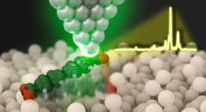
The manipulation of optical and electrical properties at the nanoscale has been critical for the development of miniaturized devices such as single-molecular sensors and photoswitches. Localized surface plasmons (LSPs), which are confined light waves generated at surfaces of nanomaterials, are powerful tools for building optoelectronic devices, as they enable reaction pathways that are inaccessible with far-field light. Traditionally, metallic structures have been targeted for LSP-induced photochemistry, which has not expanded the application of this technology to more promising platforms for nano-optoelectronics, such as semiconductor substrates.
In their recent work published in Nature Communications, the Atomic-Scale Microscopy & Spectroscopy group demonstrated the atomic-precision control of plasmon-induced single-molecule switching on a silicon surface using laser-coupled scanning tunneling microscopy. A single perylene-3,4,9,10-tetracarboxylic dianhydride (PTCDA) molecule works as a photoswitch by toggling between the silicon surface and a silver tip, triggered by LSPs at the tip excited by visible laser irradiation. This process involves the reversible breaking and formation of O–Si bonds between the molecule and the surface, as characterized with the simultaneous conductance measurement and tip-enhanced Raman spectroscopy (TERS). They achieved precise control over the reaction dynamics by adjusting the gap distance of the silver tip from the molecule in the order of 10 picometers. Their findings suggest that metal–single-molecule–semiconductor nanojunctions could serve as a versatile platform for nano-optoelectronics, or even beyond, reaching the realm of picoscale control.